H-1B Visa’s Impact Semiconductor Projects
H-1B Visa Constraints and U.S. Semiconductor Construction: Impact and Key Roles
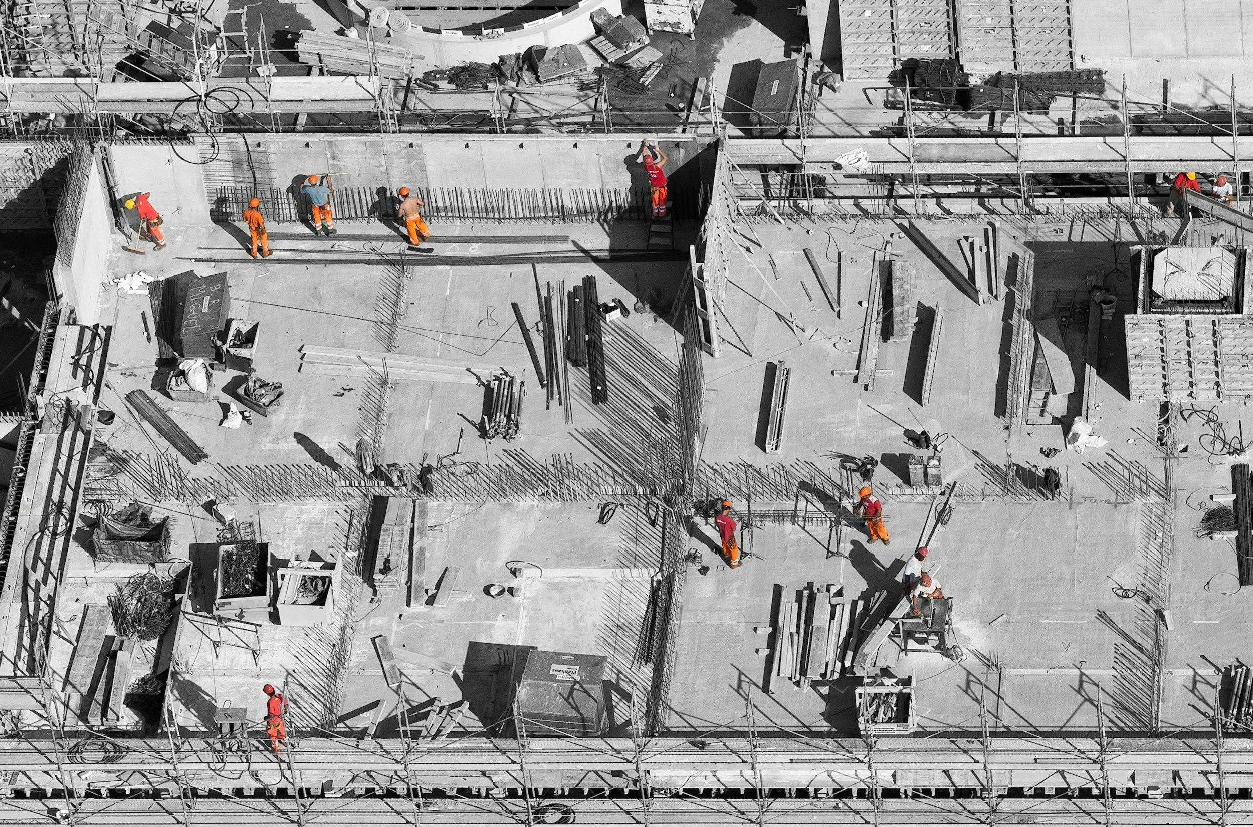
The U.S. semiconductor manufacturing boom – driven by initiatives like the CHIPS Act – has sparked a surge in new chip fabrication plants (fabs) and infrastructure projects. Yet a critical challenge looms: a shortage of skilled construction specialists to plan and build these advanced facilities[1][2]. U.S. industry leaders warn that, by 2030, tens of thousands of additional engineers and high-skill workers will be needed for semiconductor manufacturing, including fab construction[2]. In the short term, companies must often look overseas for talent. However, the H-1B visa program’s cost and policy limitations are constraining access to these foreign specialists, impacting project timelines and workforce development.
Visa Policy Limitations Strain Fab Projects
The H-1B visa, the primary U.S. work visa for high-skilled professionals, is capped at 85,000 new visas per year and subject to a lottery system[3]. These limits mean many employers cannot secure needed specialists when they need them. Timing is critical in mega-projects like fabs, but “on average, filling a semiconductor engineering role takes around 87 days” – far longer than in other tech fields[4]. This indicates a thin talent pool, and if a foreign worker loses a job, the standard 60-day visa grace period is often insufficient to find a new one, forcing skilled people to leave mid-project[4]. Strict annual caps and per-country limits further hamper predictability[5][6].
High visa costs have added another barrier. In late 2025, a new policy imposed a massive $100,000 supplemental fee for each new H-1B petition[7]. This tenfold fee hike – intended to push employers to “hire domestic talent”[7] – has alarmed industries that rely on specialized foreign workers. Such costs could make hiring needed experts “financially unworkable” for many firms[8]. For construction contractors and chip manufacturers operating on tight budgets and timelines, the fee creates a stark choice: delay projects waiting for U.S. hires who may not exist, or pay a prohibitive premium for foreign talent.
Recent high-profile semiconductor projects illustrate what’s at stake. Taiwan’s TSMC, building a $40 billion fab in Arizona, cited an “insufficient amount of skilled workers” as a reason for construction delays[9]. In mid-2023, TSMC moved to bring in 500 skilled technicians from Taiwan on visas to install specialized equipment and keep the project on schedule[10]. This drew criticism from labor unions, who noted the CHIPS Act’s intent to create American jobs[11]. But industry advocates argue that without immigration solutions, projects will falter. As one expert noted, companies building U.S. fabs have found “it’s harder to find workers than we thought”, and if the talent gap isn’t filled, new fabs may be built in the U.S. but the expertise and innovation will remain abroad[12][13].
To meet immediate needs, policymakers and industry groups have floated ideas like a special “Chipmaker’s Visa” to bypass H-1B hurdles[14][15]. While such proposals are debated, the current reality is that H-1B constraints are already affecting schedules and costs for fab construction. Below, we rank and describe the top 10 construction-related roles in semiconductor facility projects most impacted by H-1B visa issues. These roles are crucial to planning and building fabs, and many U.S. employers report shortages in each category.
Top 10 Construction Roles Affected by H-1B Visa Limits
Construction Project Managers: Fab construction projects – often multi-billion-dollar endeavors – rely on experienced project managers to coordinate architects, engineers, contractors and equipment vendors. Such expertise is scarce domestically, especially for cutting-edge chip facilities. Companies have sponsored H-1B visas for construction management professionals (over 300 H-1B positions for construction managers were certified in just two quarters of 2023)[16]. Visa caps and fees make it harder to bring in veteran project managers from overseas, potentially leading to oversight gaps and slower project delivery.
Structural Engineers: Semiconductor fabs require complex structural engineering to support massive cleanrooms and vibration-sensitive equipment. Structural engineers (often a subset of civil engineering) must design foundations and frames that meet stringent seismic and stability criteria. U.S. fab booms have strained the pool of structural specialists. H-1B visa limits impede hiring foreign structural engineers with niche expertise in high-tech facilities. (Notably, civil engineers, which include structural engineers, accounted for ~1,427 certified H-1B positions in early 2023[17].)
Electrical Engineers: Fabs consume enormous power and have intricate electrical distribution, backup, and control systems. Electrical engineers skilled in high-voltage supply, power management, and factory automation are in high demand. They are one of the most common H-1B occupations in the semiconductor industry[18]. In the first half of FY2023, U.S. employers certified roughly 3,000 electrical engineer H-1B positions[19]. Visa lottery unpredictability and new fees directly affect whether companies can hire needed electrical engineers from abroad, potentially delaying power system installation and testing.
Mechanical (HVAC/Cleanroom) Engineers: Advanced chip fabs rely on extensive HVAC, ultra-pure air and water systems, and environmental controls. Mechanical engineers design the cleanrooms, climate control, and ventilation systems that keep dust and particles at bay. This specialty is critical and in short supply – nearly 4,000 mechanical engineer H-1B positions were certified in just six months of 2023[20]. Without access to global talent (for instance, experts in cleanroom HVAC or vacuum systems), projects risk delays in achieving the strict environmental specs required for chip production.
Civil Engineers (Site and Infrastructure): Civil engineers plan the site preparation, grading, utilities, and structural layout for fab campuses. They ensure proper drainage, roads, and integration of the fab with local infrastructure. The U.S. construction labor crunch extends to civil engineering; industry-wide, civil engineers are among roles filled via H-1B visas[21]. Limitations on work visas can slow the initial phases of fab construction – from obtaining permits to completing site work – especially in regions where multiple projects compete for the same engineers[22].
Chemical/Process Facilities Engineers: Semiconductor manufacturing involves hazardous chemicals, ultra-pure water, and specialized gases. Engineers (often chemical or process engineers) are needed to design and build on-site chemical handling systems, gas distribution networks, and waste treatment facilities. These roles require specialized knowledge of chemical safety and high-purity process piping. U.S. talent in this niche is limited, so firms often look to foreign experts. H-1B data shows hundreds of chemical engineers being sponsored (e.g. ~357 in one half-year)[23]. Tight visa quotas and high fees make it harder to import chemical facilities engineers, potentially causing bottlenecks in equipping fabs with necessary chemical infrastructure.
Industrial & Logistics Engineers: Building a fab on schedule also depends on experts in logistics, scheduling, and workflow planning. Industrial engineers and logistics specialists optimize construction sequencing, coordinate the delivery of millions of dollars in tools and materials, and design efficient layouts for factories and support buildings. These skillsets are stretched thin as multiple fab projects run in parallel. H-1B visas commonly support hiring of industrial and logistics engineers in the semiconductor sector[18]. For example, over 1,500 H-1B approvals for logistician roles occurred in two quarters of 2023[24]. When visa policies constrain hiring, companies face delays in procurement and project scheduling, as the available domestic workforce may not meet the surge in demand for these planners[21].
Semiconductor Equipment Installation Specialists: A fab isn’t complete until the manufacturing tools – lithography scanners, etchers, deposition machines, etc. – are installed and qualified. Installing this highly specialized equipment often requires experts with hands-on experience from prior fab builds. Many are foreign specialists (sometimes employed by the equipment suppliers or overseas fabs). Visa hurdles have already caused issues: TSMC’s chairman noted a lack of skilled installation technicians in the U.S., necessitating foreign workers to avoid delays[25]. H-1B constraints (and related visas like L-1) directly affect whether companies can bring in these experts. If firms cannot import, say, a team of experienced tool installers, equipment commissioning can be delayed by months, holding up production ramps[10].
Architects (Fab Facility Design): Designing a semiconductor plant is a specialized branch of architecture. Architects must plan massive cleanroom spaces, chemical storage areas, and technical support buildings that comply with both industrial codes and chipmaking requirements. Because few fabs were built in the U.S. in past decades, there are limited domestic architects with this experience. Some firms have turned to international talent – indeed, nearly 500 architectural positions were filled via H-1B in a two-quarter period[26]. H-1B caps and fees make it harder for U.S. companies to hire architects who have designed fabs abroad. This can slow down the design phase or result in suboptimal layouts, impacting efficiency and cost in the long run.
Commissioning & Validation Engineers: As construction wraps up, commissioning engineers test and certify that building systems (power, HVAC, water) and production equipment meet performance specs and safety standards. Validation engineers (a role for which U.S. companies used ~1,443 H-1B positions in early 2023) ensure the cleanroom and tools achieve the stringent conditions required for chip manufacturing[27]. These experts often have deep experience in semiconductor facilities and may be brought in from overseas if not available locally. If visa restrictions prevent hiring foreign commissioning/validation engineers, new fabs could face longer debug and qualification periods before they can fully ramp up production – a costly delay for eager chipmakers.
In summary, U.S. semiconductor fab construction is acutely feeling the squeeze from H-1B visa limitations. The sector’s workforce needs are extraordinary – spanning highly educated engineers to seasoned project managers – and domestic supply alone is struggling to keep up[2][1]. Immigration policies that impose rigid caps, lengthy lotteries, and exorbitant fees are exacerbating workforce shortages at the worst time. Employers building fabs report difficulty filling roles ranging from “tech mechanical engineer[s]” to “logistics specialist[s]”, with hiring times far exceeding normal benchmarks[21]. Inability to timely source talent can translate to construction delays, cost overruns, or even decisions to scale back U.S. projects.
Industry groups and policymakers are watching these trends closely. Many advocate modernizing immigration rules – for example, extending H-1B grace periods, raising caps, or creating a tailored visa for chip industry workers[6][15]. As one CEO put it, “fixing our immigration policies” is the “low-hanging fruit” to help build the semiconductor workforce[28]. By easing H-1B restrictions and costs, the U.S. can more readily attract the specialized construction talent needed to ensure new fabs are built on time and on budget – ultimately strengthening America’s semiconductor supply chain and competitiveness[29][12].
Sources: The analysis above is supported by data and statements from industry reports and news: workforce projections by the Semiconductor Industry Association[2], expert commentary on visa policy impacts[21][7], H-1B visa usage statistics for relevant occupations[30][16], and real-world case studies such as TSMC’s Arizona fab experience[10]. These sources underscore the critical link between immigration policy and the success of U.S. semiconductor manufacturing initiatives.
[1] [22] Reshoring Semiconductor Manufacturing: Addressing the Workforce Challenge
https://www.csis.org/analysis/reshoring-semiconductor-manufacturing-addressing-workforce-challenge
[2] [12] [29] Keep CHIPS on Track
https://www.city-journal.org/article/keep-chips-on-track
[3] [18] U.S. visa options for foreign nationals in the semiconductor industry | BAL Immigration Law
[4] [5] [6] [13] [15] [21] [28] Visa Shakeup On Tap To Help Solve Worker Shortage
https://semiengineering.com/visa-shakeup-on-tap-help-solve-worker-shortage/
[7] H-1B shock: Has the US got enough of its own techies? - The Economic Times
[8] A Look at National Interest Exceptions and the $100,000 H-1B Fee | Insights | Holland & Knight
[9] TSMC delays $40B Arizona chip factory again | Construction Dive
https://www.constructiondive.com/news/tsmc-deal-arizona-labor-union-chip-factory/704847/
[10] [11] TSMC Faces Challenges in Building New Semiconductor Plant in Arizona - Lessons on U.S. FDI Attraction
[14] [25] The Chipmaker’s Visa: New Solution to Labor Shortage - Greater Phoenix In Business Magazine
https://inbusinessphx.com/economy-trends/the-chipmakers-visa-new-solution-to-labor-shortage
[16] [17] [19] [20] [23] [24] [26] [27] [30] H-1B Selected Statistics, Fiscal Year 2023 Q1&Q2 (October 1, 2022 through March 31, 2023)