SK hynix Commits $13 Billion to Advanced Chip Packaging and Testing Hub
The new facility will focus on high-end packaging and testing technologies required for next-generation memory products, particularly high-bandwidth memory (HBM) used in artificial intelligence accelerators and data-center processors.
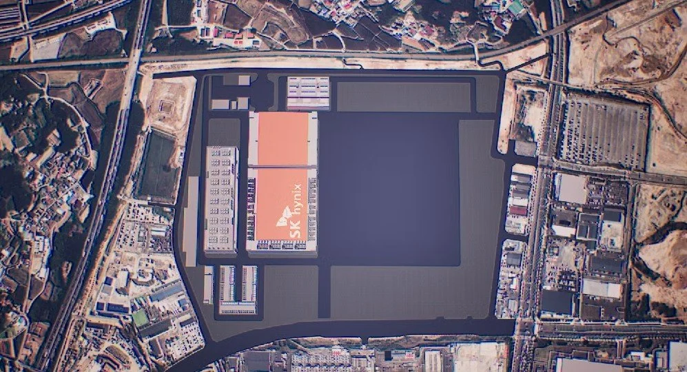
SK hynix has unveiled plans to invest nearly $13 billion in a new advanced semiconductor packaging and testing facility in Cheongju, South Korea, underscoring the company’s determination to strengthen its position at the center of the global AI memory supply chain. The project represents one of the largest single investments ever made in chip packaging infrastructure and highlights how critical advanced packaging has become as the semiconductor industry pushes beyond conventional scaling.
The new facility will focus on high-end packaging and testing technologies required for next-generation memory products, particularly high-bandwidth memory (HBM) used in artificial intelligence accelerators and data-center processors. As AI workloads grow more complex, the performance gains increasingly come not only from the silicon itself but from how chips are stacked, interconnected, and integrated. SK hynix’s investment reflects this shift, positioning packaging as a strategic differentiator rather than a back-end afterthought.
Cheongju was selected as the site for the expansion because it already hosts significant SK hynix operations and offers established infrastructure, skilled labor, and proximity to suppliers. The project will be developed in stages, with construction beginning in the second half of the decade and operations ramping up toward the end of the 2020s. Once complete, the complex is expected to employ thousands of workers and play a central role in scaling production of AI-focused memory solutions.
The timing of the investment is closely tied to booming demand for AI hardware. SK hynix is currently the leading supplier of HBM used in advanced AI chips produced by companies such as Nvidia, and capacity constraints across the industry have turned advanced packaging into a bottleneck. By expanding its domestic packaging and testing capabilities, SK hynix aims to secure tighter control over supply, shorten production cycles, and maintain technological leadership as competition intensifies.
The South Korean government has welcomed the project, viewing it as a cornerstone investment that reinforces the country’s semiconductor ecosystem. The facility aligns with broader national efforts to keep high-value semiconductor manufacturing anchored in Korea, particularly in areas such as memory, materials, and advanced processes where the country already enjoys global leadership. Local authorities in Cheongju also expect the project to stimulate regional development through job creation and supplier growth.
Industry analysts see the move as a clear signal that the next phase of semiconductor competition will be fought as much in packaging and integration as in wafer fabrication. Technologies such as 3D stacking, hybrid bonding, and advanced testing are becoming essential to deliver the bandwidth, power efficiency, and reliability required by AI and high-performance computing systems. SK hynix’s willingness to commit $13 billion to this segment highlights how strategic these capabilities have become.
When fully operational, the Cheongju facility will serve as a backbone for SK hynix’s AI memory roadmap, enabling the company to scale production of increasingly complex HBM products and reinforcing South Korea’s role as a global semiconductor powerhouse. In an era defined by AI-driven demand and supply-chain resilience, the investment marks a decisive step in ensuring that advanced packaging keeps pace with the industry’s most ambitious technological goals.
Project News