SK hynix to Launch Construction of $3.9b Indiana Chip Packaging Facility
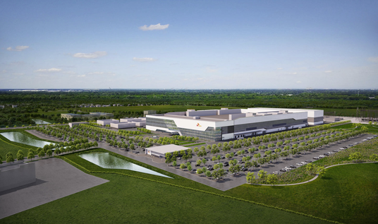
A designer's drawing of SK hynix's advanced semiconductor packaging plant in West Lafayette, Indiana
SK hynix is set to begin construction of its $3.87 billion advanced semiconductor packaging plant in Indiana later this month, marking a major step in the company's efforts to expand its artificial intelligence chip production capacity in the United States.
According to industry sources, the South Korean memory chip manufacturer will hold a groundbreaking ceremony on Aug. 27 in West Lafayette, Indiana, where it is developing an advanced packaging facility and high-bandwidth memory (HBM) research center. Invitations have already been sent to key customers and business partners.
The event is expected to draw senior SK Group leaders, including Chairman Chey Tae-won and SK hynix CEO Kwak Noh-jung, along with executives from major technology firms and supply chain partners.
The ceremony could also provide another opportunity for Chey to meet Nvidia CEO Jensen Huang, although Huang's attendance has not yet been confirmed. The two executives have met several times recently as SK hynix strengthens its partnership with Nvidia in the rapidly growing AI and HBM markets.
The groundbreaking is also likely to highlight the company's broader ambitions in the US. Following SK hynix's US depositary receipt listing last month, Chey indicated that the company is evaluating additional investments beyond the Indiana facility. He noted that a US-based memory manufacturing plant remains a possibility if critical requirements such as power availability, water resources, workforce access, and supply chain infrastructure can be secured.
SK hynix first announced the Indiana project in 2024, committing $3.87 billion to build an advanced chip packaging plant and research and development center near Purdue University.
The facility is scheduled to begin mass production in the second half of 2028. It will focus on packaging HBM chips, a crucial memory technology that stacks multiple DRAM chips to provide the high data bandwidth needed for AI processors.
The project has received significant support from the US government through the CHIPS Act, which includes up to $450 million in direct funding and an additional $500 million in loans.
Site preparation and concrete work started earlier this year, while the Aug. 27 ceremony is expected to signal the start of full-scale construction.
Once operational, the Indiana plant will establish SK hynix's US manufacturing base for advanced HBM packaging, positioning the company to better serve growing demand for AI-focused memory solutions.

Project News