$5b investment creates the world’s largest semiconductor R&D facility
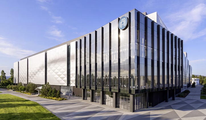
Applied Materials Unveils $5 Billion EPIC Center in Silicon Valley
Applied Materials Unveils $5 Billion EPIC Center to Accelerate Chip Innovation
Applied Materials has unveiled its Equipment and Process Innovation and Commercialization (EPIC) Center, a $5 billion investment in collaborative semiconductor research and development. Located at the company’s Sunnyvale, California, campus, the center brings chipmakers, system designers, equipment suppliers and university researchers together to develop technologies for the AI era.
Applied describes EPIC as the world’s largest facility dedicated to collaborative R&D in semiconductor process technology and manufacturing equipment. Its goal is to shorten the journey from materials research to high-volume chip production as AI drives demand for more powerful, energy-efficient computing.
“As AI infrastructure scales, the demands of high-performance computing are driving unprecedented complexity across the chipmaking roadmap,” said Gary Dickerson, president and CEO of Applied Materials.
Dickerson said meeting those demands requires the industry to rethink how it develops and commercializes semiconductor technologies. EPIC is designed to support that shift by placing partner teams alongside Applied’s scientists and engineers.
Bringing Research and Manufacturing Development Together
Semiconductor development has traditionally moved through separate stages: foundational materials research, equipment and process development, then integration and pilot production. Each transition requires a handoff between teams and facilities.
EPIC brings those activities into one location. Researchers who develop materials, engineers who build equipment and manufacturers who produce chips can work together throughout the development process, identifying problems earlier and refining technologies with commercialization in mind.
Dr. Prabu Raja, president of Applied’s Semiconductor Products Group, said atomic-scale dimensions have made materials and their interfaces increasingly complex. Addressing those challenges requires coordinated development across materials, processes and equipment.
By involving customers’ engineers before technologies reach their factories, Applied expects EPIC to help chipmakers achieve strong performance and production yields sooner.
The operating model also gives Applied greater visibility into customers’ technology roadmaps. That insight can guide its R&D spending and help the company develop equipment and services suited to future manufacturing needs.
A Facility Built for Large-Scale Collaboration
The 600,000-square-foot EPIC Center contains nearly four acres of advanced cleanroom space and took more than six million construction hours to complete.
The building’s foundation contains enough concrete to fill 34 Olympic-sized swimming pools, while its structure uses enough steel to build two Eiffel Towers. Above the cleanrooms, 34 roof trusses each span nearly 300 feet and weigh as much as 12 school buses.
Applied says the scale reflects the technical demands of semiconductor R&D and the need to accommodate multiple partners working through closely coordinated, secure development cycles.
Partners Across the Semiconductor Industry
EPIC’s founding partners are TSMC, Intel, SK hynix, Micron and Samsung Electronics.
They are joined by innovation partners Broadcom, Advantest, SCREEN, KIOXIA and BE Semiconductor Industries, known as Besi. Academic research partners include Arizona State University, Rensselaer Polytechnic Institute, Stanford University, UC Berkeley and the UCLA Samueli School of Engineering.
Each partner will bring engineers and technology challenges into the facility to work alongside Applied’s teams. Additional companies and research organizations are expected to join over time.
The unveiling included a summit hosted by Raja, where R&D leaders from semiconductor design, manufacturing and equipment companies discussed challenges facing the global chip industry.
Advancing Logic, Memory and Packaging for AI
Partner companies highlighted several areas where closer collaboration could accelerate development.
TSMC Chairman and CEO Dr. C.C. Wei pointed to the companies’ three-decade relationship and the growing complexity of chipmaking beyond the 2-nanometer node. He said early access to new equipment technologies could help advance energy-efficient AI architectures, low-resistance wiring and advanced packaging.
Intel CEO Lip-Bu Tan emphasized the need for continued progress in transistors, interconnects and packaging. With Intel targeting more than a trillion transistors in a package by 2030, he said closer work with equipment partners could improve R&D efficiency and speed the introduction of new technologies.
Memory manufacturers focused on the demands of data-intensive AI workloads. Micron Chairman and CEO Sanjay Mehrotra said EPIC would help move next-generation memory technologies from research into large-scale production. SK hynix President and CEO Nohjung Kwak highlighted opportunities across high-bandwidth memory, DRAM and NAND to improve the bandwidth, speed and capacity needed to keep powerful processors supplied with data.
Samsung’s Device Solutions CTO, Jaihyuk Song, said collaboration would span leading-edge logic, memory and advanced packaging.
Other partners emphasized the connections between chip design, manufacturing and system performance. Broadcom identified advanced packaging as essential to integrating compute, memory and connectivity. Advantest highlighted the value of linking process development with testing and measurement to improve yields and production ramps.
SCREEN said closer coordination of wet and dry processes could support increasingly complex 3D devices and packaging structures. KIOXIA pointed to collaboration across memory, logic and interconnect technologies, while Besi emphasized hybrid bonding as a foundation for high-performance 3D integrated devices.
Together, these efforts reflect EPIC’s central premise: the semiconductor technologies needed for AI require coordinated advances across the industry. Applied is betting that bringing those capabilities under one roof will help turn promising research into production-ready technology faster.

Project News