Building the Future: What It Takes to Create an Advanced Semiconductor Packaging Facility
Traditionally, chips were packaged individually and then assembled onto circuit boards.
When people think about semiconductors, they usually picture ultra-clean factories producing tiny chips etched onto silicon wafers. But increasingly, the real innovation—and competitive advantage—is happening after the chip is made. This is where advanced packaging comes in, and it’s why companies like Intel are investing heavily in it as a key differentiator.
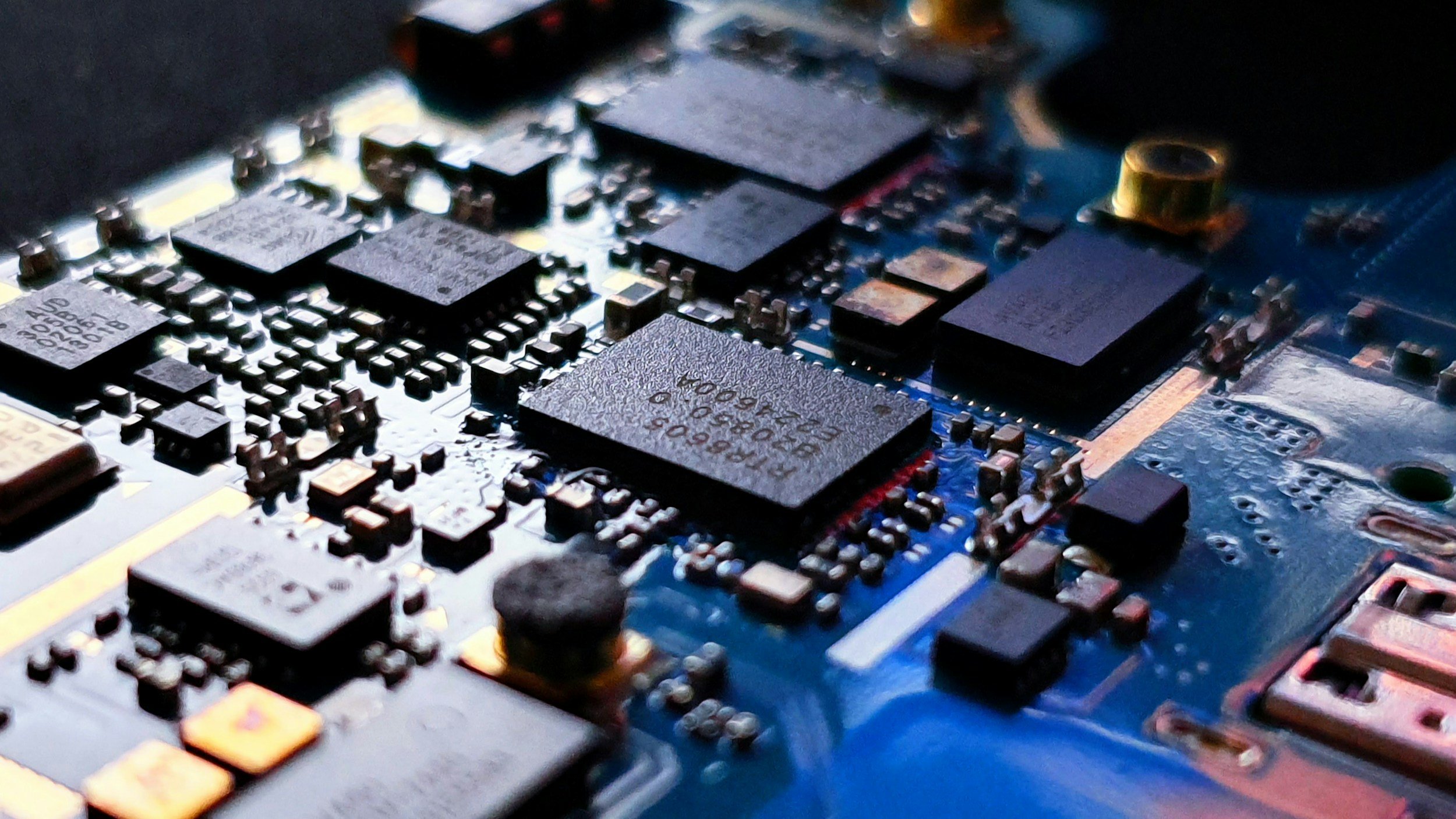
Traditionally, chips were packaged individually and then assembled onto circuit boards. Advanced packaging changes that by combining multiple chips—sometimes from different manufacturers—into a single, highly integrated unit. This allows for faster performance, lower power consumption, and more compact devices. A helpful way to think about it is moving from single Lego blocks to fully assembled modules that snap into place instantly.
The first step in building an advanced packaging facility is selecting the right location. While these facilities are not quite as resource-intensive as full semiconductor fabrication plants, they still demand robust infrastructure. Reliable power is essential, often with backup systems to prevent any interruptions. Access to high-quality water is also important for cleaning and processing steps. Strong transport links are needed to move sensitive components efficiently, and the ground conditions must support highly precise equipment. Just as critical is proximity to an existing semiconductor ecosystem, including suppliers, customers, and a skilled workforce.
Inside the facility, the environment must be tightly controlled. Advanced packaging involves making microscopic connections between components, so even a tiny particle of dust can cause defects. This requires the construction of cleanrooms where air quality is carefully filtered and monitored. Temperature and humidity must be kept within strict limits, and the building itself must minimize vibrations that could disrupt delicate alignment processes. Although these standards may not always reach the extreme levels of leading-edge chip fabs, they are still among the most stringent in manufacturing.
The technology inside the facility is where much of the complexity—and cost—lies. Advanced packaging relies on highly specialized equipment to bond chips together, connect them vertically, and ensure precision at every stage. These machines are often sourced from a limited number of global suppliers and can take months or even years to procure and install. The integration of this equipment into a seamless production line is a major engineering challenge in itself.
Equally important is the workforce needed to operate the facility. Advanced packaging requires a blend of highly skilled engineers, technicians trained in cleanroom environments, and specialists in materials and quality control. This is not traditional manufacturing; it is precision engineering at the nanoscale. As a result, companies often need to invest heavily in training programs and partnerships with universities to build a sustainable talent pipeline.
No facility operates in isolation, and advanced packaging is especially dependent on a strong supply chain. A steady flow of substrates, specialty chemicals, and precision components is required to keep operations running smoothly. In addition, testing and validation services play a critical role in ensuring that the final products meet strict reliability standards. Establishing this ecosystem locally, or ensuring efficient global logistics, is a key part of any successful project.
Behind the scenes, the facility depends on significant utility infrastructure. Electricity powers both the production equipment and the environmental control systems that keep conditions stable. Ultra-pure water systems are needed for cleaning processes, while waste treatment facilities must safely handle chemical byproducts. Data infrastructure is also essential, enabling real-time monitoring and automation of highly complex processes. While these requirements are somewhat less demanding than those of a full fabrication plant, they are still substantial and must be designed with reliability in mind.
From an investment perspective, advanced packaging facilities are more accessible than traditional fabs but still represent a major financial commitment. Projects typically range from a few billion to around ten billion dollars, depending on their scale and technological sophistication. Construction can take several years, followed by an additional period to ramp up production and achieve full operational efficiency. This relatively lower barrier to entry is one reason why governments and companies are increasingly focusing on packaging as a strategic opportunity.
Ultimately, advanced packaging is becoming one of the most important frontiers in the semiconductor industry. As the pace of shrinking transistor sizes slows, performance improvements are increasingly driven by how chips are combined rather than just how small they are. For regions looking to establish themselves in the semiconductor space, advanced packaging offers a compelling pathway. It brings significant job creation, supports the development of a broader technology ecosystem, and provides a foothold in a critical global industry.
Building such a facility is undoubtedly complex, requiring careful coordination of infrastructure, technology, talent, and supply chains. Yet it is also an achievable and highly strategic investment. As companies like Intel continue to push the boundaries of what advanced packaging can deliver, these facilities are set to play a central role in shaping the future of computing—quietly enabling the devices and systems that power our everyday lives.

Project News