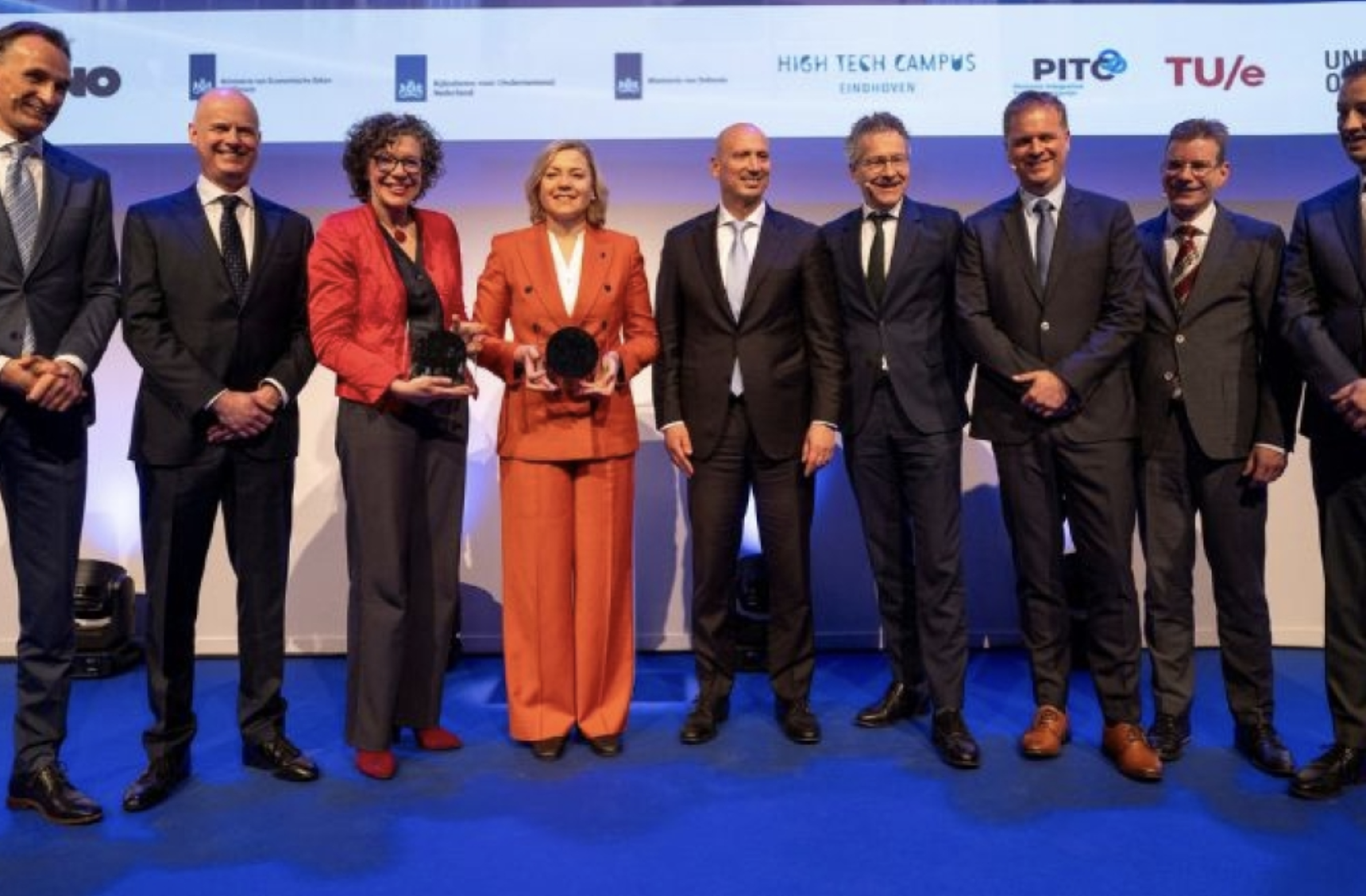
Fab begins construction in Eindhoven
€150 million European Chips Act investment in Eindhoven…
Netherlands Organisation for Applied Scientific Research (TNO) and High Tech Campus Eindhoven have begun construction of a new pilot foundry designed to produce indium phosphide (InP) photonic chips on a 6-inch wafer scale, marking an important step in Europe’s efforts to strengthen its semiconductor capabilities.
The new facility will bridge the gap between research and large-scale manufacturing, enabling faster development of photonic technologies and accelerating their transition from laboratory concepts to commercial products. These technologies are expected to play a key role in powering next-generation energy-efficient AI data centres, 6G communications networks, medical innovations and advanced supercomputing systems.
Tjark Tjin-A-Tsoi, CEO of TNO, said the project represents a major milestone for the organisation. He explained that the facility will serve as an industrial pilot line, bringing research and manufacturing closer together while helping companies scale up high-quality photonic chip production more efficiently. According to Tjin-A-Tsoi, the investment will strengthen the Netherlands’ role within the European semiconductor ecosystem while supporting future economic growth.
The project involves an investment of approximately €150 million, supported by the ambitions of the European Chips Act. The foundry will also operate as part of the wider European consortium PIXEurope, which aims to ensure that critical semiconductor technologies underpinning the digital economy are developed and manufactured within Europe.
The initiative is being delivered through a public-private partnership involving TNO, Eindhoven University of Technology, PhotonDelta, SMART Photonics and High Tech Campus Eindhoven.
Beyond advancing semiconductor innovation, the facility is also expected to generate skilled employment. Around 40 specialists will be employed during the initial phase, with further expansion anticipated as production scales.
Peter Wennink, a technology adviser to the Dutch government, said the rise of integrated photonics could have an impact comparable to the emergence of integrated electronics decades ago. By investing in scalable manufacturing today, he said Europe is laying the groundwork for a new technology ecosystem capable of shaping the future of the global digital economy.

Project News