Looking back at 2025 projects….
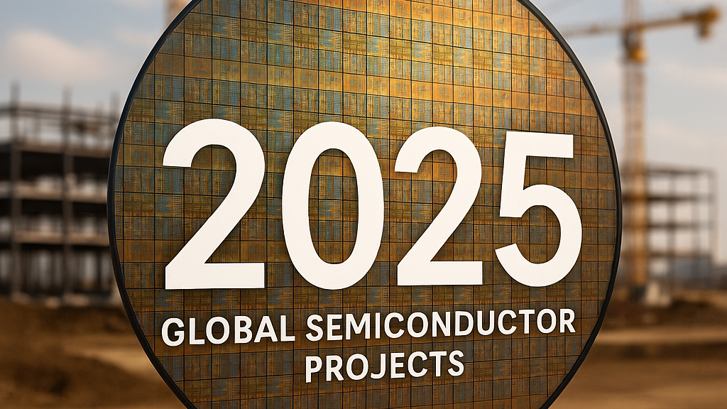
Worldwide semiconductor projects in 2025 review - what is next in 2026….. GSP Looks Back
What a crazy year 2025 was for the Semiconductor construction industry. Across the U.S., Europe, and APAC, the year has seen dozens of fab announcements, strategic delays, major government subsidies, and acceleration in advanced packaging and materials manufacturing. Giants of the industry have fallen and risen up again, Fab's have swapped hands, new countries have emerged as semiconductor hubs and the advancement in AI and Data centers has driven the need for semiconductors through the roof, and it looks to continue into 2026.
JANUARY 2025
Global Build Momentum & Early Market Signals
The year started with strong expansion activity from major global players including TSMC, Intel, Samsung, GlobalFoundries, Texas Instruments, and Micron. Micron stood out as the most aggressive builder, announcing new greenfield projects and expansions across New York, India, Singapore, Boise, Manassas, and Japan. Europe showed positive progress with ESMC and Infineon advancing on schedule, while Silicon Box, GlobalWafers, and IMEC all moved into new approval or design phases. At the same time, Wolfspeed and STMicro signalled industry challenges tied to EV and power-electronics demand slowdowns, marking an early indication of market trends.
FEBRUARY 2025
Intel Delays Ohio Megaproject by 3 Years
Intel delivered one of the first major shocks of the year by pushing out its Ohio megafab timeline. Originally expected to be completed in 2027, the first module is now forecasted for 2030–2031, with the second module coming about a year later. While this delay underscores the company’s ongoing restructuring, former CEO Craig Barrett publicly defended Intel’s long-term trajectory, insisting that the company remains far from broken and is positioned for recovery.
Major European Funding Approvals
Europe saw significant financial and political momentum as AMS OSRAM secured €227 million in EU Chips Act support to strengthen its Austrian site, while Black Semiconductor raised €254 million for a graphene-based chip facility in Aachen, Germany. These projects reflected Europe’s push into next-generation semiconductor materials and photonics, reinforcing its goal to secure a resilient regional supply chain.
US R&D & Fab Acquisition Activity
The U.S. added momentum through major research and manufacturing initiatives, including Penn State’s announcement of a new semiconductor research facility aimed at boosting academic–industry collaboration. Apple committed to investing $500 billion in the U.S. with a large AI server factory in Texas, while SkyWater purchased Infineon’s Austin Fab 25 to expand domestic 200mm chip production. Collectively, these efforts strengthen the U.S. innovation ecosystem.
TSMC, SK Hynix, GF & Quantinuum Advance U.S. Plans
TSMC signalled accelerated planning for a third fab in Arizona. SK Hynix began construction on its Yongin memory cluster, aiming to build a strong next-generation DRAM base. GlobalFoundries advanced plans for a new assembly and test facility in New York, and Quantinuum announced a New Mexico R&D centre focused on photonics for quantum computing — marking major advancements across the U.S. manufacturing landscape.
MARCH 2025
Intel & TSMC Explore Joint Venture
March brought news of a potential joint venture between Intel and TSMC — an unprecedented collaboration between two long-time competitors. This possible partnership, represented a meaningful shift in strategic alignment and underscores the U.S. government’s pressure to secure advanced domestic manufacturing capacity. It didn't happen but it caused the industry to blink.
Europe & Asia Ramp Up Materials & Production
Germany’s ESMC project continued hitting critical construction milestones to keep its 2027 production timeline on track. Silicon wafer producer Okmetic announced expansion plans to support the rising need for advanced substrates. Meanwhile, UMC formally opened its Singapore fab expansion, reinforcing its growing share of global mature-node capacity and strengthening supply-chain resilience.
UK Semiconductor Momentum
Vishay newport secured up to €250 million for a new chip production facility, reinforcing the UK's manufacturing ambitions. Government representatives highlighted Vishay’s Newport fab during an official visit, underscoring its strategic importance to national capability and job creation. In the U.S., GlobalWafers delivered its first shipment from its new plant — a milestone in domestic wafer production.
APRIL 2025
TSMC Completes Arizona Fab 2 Early
TSMC completed its second Arizona fab ahead of schedule, marking a significant victory for U.S. manufacturing. As part of a $165 billion U.S. investment program, the Phoenix mega campus aims to produce 30% of TSMC’s most advanced chips domestically. This achievement boosted confidence in America’s ability to attract and execute next generation fabs.
Samsung Delays Texas Fab to 2027
Samsung confirmed that its Taylor, Texas fab will be delayed until 2027 due to construction and supply-chain issues. The delay raised broader questions about CHIPS Act timelines and the practicality of U.S. workforce and supplier readiness. It also dimmed expectations for an immediate surge in U.S. advanced-node output.
Europe Announces New Investments & Projects
Europe continued its momentum with a major investment to restart the BelGaN chip site in Belgium, while Octric Semiconductor secured £200 million to expand design and production capacity. Catalonia announced the InnoFAB initiative, including a 2,000 m² state-of-the-art cleanroom, signalling the region’s push to become a hub for advanced semiconductor R&D and prototyping.
MAY 2025
GlobalWafers & Deposition Technology Expand in the U.S.
In the U.S., GlobalWafers America advanced plans for a new 300mm wafer facility in Texas, strengthening domestic materials independence. At the same time, Deposition Technology Inc., a subsidiary of Korea’s WONIK QnC, announced a $100 million expansion in Austin to increase semiconductor materials output. Together, these investments meaningfully reduce reliance on Asian wafer and materials supply chains.
ASML, CLAS-SiC & Jenoptik Drive European High-Tech Growth
Europe recorded several high-impact investments as ASML accelerated its massive Veldhoven expansion to support rising global demand for EUV and High-NA lithography equipment. CLAS-SiC revealed plans to build a dedicated power semiconductor fab focused on energy-efficient wide-bandgap technologies. Jenoptik launched a precision optics fab in Dresden, further strengthening Saxony’s leadership in semiconductor optics and manufacturing.
India’s Mixed Momentum in Chip Ambitions
India’s semiconductor investment environment produced both positive and negative developments. The government approved the HCL–Foxconn joint venture, considered a crucial step toward domestic chipmaking. Meanwhile, Zoho paused its $700 million project, and Adani suspended its collaboration with Tower Semiconductor, reflecting ongoing challenges in navigating geopolitics, financing, and project readiness.
TSMC Announces 9 New Facilities
TSMC rounded out the month with news of nine new global facilities slated for 2025. The company also confirmed that sub-2nm mass production will begin in Taichung by 2028, cementing Taiwan’s leadership in next-generation lithography and transistor architectures.
JUNE 2025
Wolfspeed Restructures to Refocus on SiC Growth
Wolfspeed announced a major restructuring designed to strengthen its long-term positioning in silicon carbide technologies. With SiC chips increasingly vital for EVs, renewable energy, and energy-storage systems, the company refocused resources to manage a short-term weakness in EV markets. The plan was widely interpreted as laying groundwork for future profitability and scalability.
U.S. Regional Competition Intensifies
Michigan entered the semiconductor spotlight by aggressively lobbying for new fabs in preference to Ohio, highlighting the competitive dynamic among U.S. states vying for CHIPS Act funding. SkyWater completed its acquisition of Infineon’s Austin fab, adding new domestic specialty-process capacity. Meanwhile, Micron released a detailed environmental impact statement for its New York megafab, including extensive sustainability commitments praised by local regulators.
Massive U.S. Investments from TI and GF
Texas Instruments committed more than $60 billion to expand its U.S. manufacturing footprint GlobalFoundries complemented this with a $16 billion U.S. investment drive focused on reshoring essential chip technologies and expanding its New York and Vermont facilities. Both moves reinforced the U.S.’s ambition to rebuild domestic semiconductor manufacturing.
APAC Strengthens Its Position
APAC also recorded major milestones as Tata broke ground on India’s first indigenous semiconductor fab in Gujarat, supported by workforce housing and long-term community infrastructure. Micron’s Sanand facility achieved cleanroom validation, positioning India closer to becoming a meaningful contributor to global supply. South Korea reaffirmed national investment strategies centred around AI-driven system semiconductor leadership.
JULY 2025
Intel Evaluates Shifting Advanced Manufacturing out of Oregon
Intel were rumour to be considering a strategic evaluation regarding the future of advanced manufacturing in Oregon, long home to its largest R&D and production hub. Although no decisions have been made, the prospect of shifting major functions away from the Pacific Northwest prompted significant debate about potential economic and national-manufacturing implications.
TSMC Escalates Arizona Campus Vision
In contrast, TSMC continued expanding in the U.S., unveiling plans for its Phoenix site to operate as a sprawling “city within a city.” With billions of dollars invested and multiple fabs planned, TSMC’s Arizona mega-campus has become a cornerstone of the long-term U.S. semiconductor ecosystem and a defining project for the region’s future economy.
Samsung Wins $16.5B U.S. Contract
Samsung received a major boost with a $16.5 billion U.S. government contract, one of the largest semiconductor supply deals ever awarded. The contract dramatically strengthens Samsung’s position within the U.S. market and adds urgency to its domestic manufacturing and packaging expansion strategy.
Europe & Asia Expand Infrastructure
Europe saw additional momentum as Air Liquide committed over €250 million to support semiconductor facilities across the region. Catalonia launched the INNOFAB Foundation after Spain lost a $1 billion Broadcom project, signalling a shift in regional competitiveness. Taiwan continued solidifying its leadership by announcing an 11-fab expansion plan and a nationwide AI-driven economic initiative valued at NT$510 billion.
AUGUST 2025
U.S. Government Takes 10% Stake in Intel
In a historic and controversial move, the U.S. government converted CHIPS Act grants into a 9.9% equity stake in Intel valued at about $10 billion. Supporters argued this provides Intel the financial backing necessary to regain technological leadership, while critics raised concerns about federal influence over corporate governance.
TSMC Accelerates Arizona Packaging Facilities
TSMC pushed forward with two advanced packaging plants in Arizona — AP1 and AP2 — aimed at supporting SoIC, CoW, and CoPoS technologies for AI and high-performance computing. With construction slated to begin in 2026 and production planned for 2028, these sites strengthen America’s foothold in advanced packaging.
Samsung, Micron, Apple & Amkor Intensify U.S. Expansion
Samsung considered expanding its Taylor investments beyond $50 billion, driven partly by demand from new partnerships such as its major contract with Tesla. Micron began early site prep at its $100 billion New York megafab, while Apple formally backed Texas Instruments’ Lehi expansion. Amkor announced a $2 billion advanced packaging facility in Arizona, reinforcing a rapidly growing U.S. ecosystem.
Europe & APAC Growth Continues
Europe advanced plans for a new photonics chip hub in Belgium and welcomed £100 million into the UK’s Plessey Semiconductor under its new ownership structure. In Asia, TSMC reaffirmed its commitment to a second fab in Kumamoto, ensuring Japan remains a pillar of its global diversification strategy.
SEPTEMBER 2025
U.S. Facility Sales & Restructuring
LA Semiconductor initiated the sale of its U.S. wafer fab, drawing attention amid pressure to expand onshore capacity. Wolfspeed completed its restructuring plan, significantly improving its financial outlook, while Skanska expanded its capabilities to meet rising global demand for semiconductor and data-center construction — a key bottleneck in the supply chain.
UK & Germany Announce Key Moves
Reports surfaced that IQE, one of the UK’s leading semiconductor players, may be up for sale, reflecting challenges for independent European chipmakers. Germany saw continued strength as Jenoptik expanded its optics manufacturing in Jena, supporting advanced lithography and photonics demand. STMicroelectronics also announced investments to scale its analog and power device production.
APAC Investments Accelerate
Japan approved a massive $3.6 billion subsidy for Micron’s Hiroshima DRAM fab, reinforcing its AI-driven memory roadmap. X-FAB opened a major cleanroom expansion in Malaysia, significantly increasing wafer output, while Tata Consulting Engineers deepened involvement in India’s Odisha semiconductor initiative — all contributing to APAC’s continued rise as a semiconductor powerhouse.
OCTOBER 2025
Micron Secures Key Power Infrastructure in NY
New York approved a vital 345 kV underground power line for Micron’s $100 billion megafab, marking a critical infrastructure milestone for what is expected to be the state’s largest-ever private investment. The project is projected to support more than 50,000 jobs over two decades.
GlobalFoundries Announces €1.1B Expansion
GF announced “Project SPRINT,” a €1.1 billion expansion of its Dresden fab, aiming to exceed one million wafers per year by 2028. The upgrade aligns with Europe’s strategic goals under the EU Chips Act and strengthens regional supply-chain resilience for automotive, IoT, and defense markets.
TSMC, VIS/NXP & ADI Announce APAC and EU Moves
TSMC submitted plans to build a new fab in Taichung focused on high-speed wafer production. In Singapore, VIS and NXP began construction of their new joint-venture fab, with TSMC licensing the technology. Meanwhile, Analog Devices and ASE announced a strategic partnership that includes ASE’s intent to acquire ADI’s Penang facility — reinforcing collaboration between design and packaging expertise.
Mitsubishi Electric Opens SiC Facility
Mitsubishi Electric completed its new six-story SiC power semiconductor facility in Kumamoto. While some equipment installation has been postponed to 2031 due to slower EV demand, initial operations are on track to begin in November 2025, marking a major milestone in Japan’s SiC roadmap.
NOVEMBER 2025
Micron Delays NY Megafab Schedule
Micron announced another schedule shift for its massive New York project, now expecting main construction to start in Q2 2026 and initial output in 2030. The full buildout will extend through 2041. Despite this, site preparation and infrastructure work will continue, reaffirming long-term commitment.
New U.S. SiC & Photonics Facilities Launch
The University of Arkansas opened the MUSiC facility — the nation’s only open-access SiC fab — providing a significant boost for research and prototyping. In Europe, Exyte was selected to build Black Semiconductor’s FabONE, the world’s first graphene-photonics fab, positioning Germany at the forefront of next-generation device technologies.
imec Expands Globally; GF Acquires AMF
imec revealed plans for a major new research hub in Qatar, focusing on photonics, 3D ICs, and AI-driven design tools. GlobalFoundries acquired Advanced Micro Foundry in Singapore, instantly becoming the world’s largest pure-play silicon photonics foundry. TSMC prepared to break ground on its A14 fab in Taichung, introducing its next major technology node.
Elon Musk/Tesla: Gigantic Chip Fab for AI & Robotics
Elon Musk stated that Tesla may need to build a “gigantic” semiconductor fabrication plant—referred to as “Terrafab”—to meet future AI and robotics chip demand that external suppliers might be unable to satisfy. The proposed fab could start at ~100,000 wafer starts per month and scale up to ~1 million, underscoring Tesla’s ambitions to vertically integrate chip production for its autonomous and AI hardware. (Watch this space)
December 2025
EU Commission approves €1 Billion in aid
The European Commission has approved €623 million in German state aid to help build two new semiconductor manufacturing facilities in Dresden and Erfurt. GlobalFoundries receives €495 million to expand 300 mm wafer production. X-FAB gets €128 million for a new open foundry at its Erfurt site. These projects, supported under the European Chips Act, aim to strengthen the EU’s technological autonomy and semiconductor supply chain. The EU approved an additional €450 million subsidy from the Czech government for onsemi’s new silicon carbide (SiC) fab in Rožnov pod Radhoštěm.
$614 Million New York NanoFab
In Albany, New York, the NanoFab Reflection facility has reached a topping-out milestone. The $614 million cleanroom building will house advanced research and fabrication space, anchoring the New York CREATES complex and reinforcing the region’s role in chip manufacturing.
$5.16 Billion Chip Investment Projects in Oman
Oman announced three semiconductor investment opportunities totaling about $5.16 billion aimed at diversifying its tech ecosystem: This will include a semiconductor design company, a Middle East OSAT (outsourced assembly and testing) facility and a large silicon raw material plant These initiatives are designed to attract global partners and enhance Oman’s role in the global semiconductor value chain.
Wolfspeed Receives $698.6 Million
To continue the amazing Wolfspeed recovery story, Wolfspeed received $698.6 million in cash tax refunds from the U.S. Internal Revenue Service under the Advanced Manufacturing Investment Credit (AMIC). The refund boosts its cash balance to around $1.5 billion, improving liquidity. Funds will be used to retire debt and support the ramp-up of its 200 mm SiC wafer manufacturing, critical for EV power electronics, AI data centers, aerospace and defense, and industrial energy markets.
In summary
2025 was a defining year for semiconductor manufacturing, characterised by historic megafab commitments, structural reorganisations, record-breaking public incentives, and intense global competition for capacity and talent. AI demand continues to fuel unprecedented investment levels, even as the EV and power-electronics markets experience cyclical headwinds. The decisions made in 2025 — in funding, technology choice, and international partnerships — will shape global semiconductor landscapes for decades to come.
Project News