RnD Fabs on the Rise
Texas A&M Semiconductor Institute
Over the past decade there has been a global surge in building specialized semiconductor research-and-development (R&D) fabrication facilities at universities and public institutes. These facilities – often called “R&D fabs” or pilot lines – are funded by a mix of government and academic investment. According to recent reports, new expansions in R&D fabs represent some of the first since the mid-2010s. For example, a 2025 news brief noted that New York’s Albany NanoTech Complex is launching its first major expansion since its 2015 project. In Europe, chip research hubs are also expanding; in 2024 the Belgian research center IMEC announced plans for a new 300mm pilot line in Málaga. Together these developments illustrate how both national governments and universities all over the world have ramped up semiconductor research facilities since 2010.
U.S. University and State Initiatives
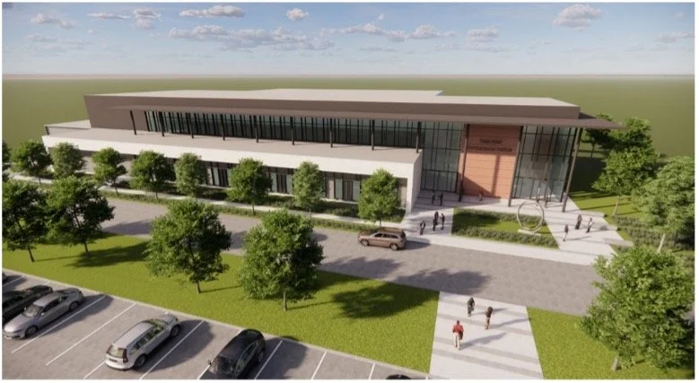
In the United States, state governments and universities are investing hundreds of millions in such R&D fabs. For example, Texas A&M University is building a dedicated semiconductor institute at its RELLIS research campus, slated to open in early 2028. According to the Texas A&M Semiconductor Institute, the new facility will include a Class-100 clean room with 300mm processing tools and advanced packaging labs.
The State of Texas approved about $226.4 million for this project. Local news reports confirm that construction of the roughly 70,000 ft² building (initial phase ~$205 M) will begin in 2026, with most of the work to be completed by 2028. These developments are intended to cement Texas’s role as a leader in semiconductor research and workforce training.
In Arizona, the state’s three public universities have likewise launched new chip R&D centers. According to the Arizona Board of Regents, Arizona State University (ASU), Northern Arizona University (NAU), and the University of Arizona (UA) have become central to the state’s semiconductor strategy. ASU recently opened a $270 million “Materials-to-Fab” Center in Tempe to support advanced packaging and materials science research. State funding also enabled facilities at the other campuses: ASU received an additional $47.5 M, NAU got $13 M to build a semiconductor workforce training lab in Phoenix, and UA received $35.5 M to expand its Micro/Nano Fabrication Center in Tucson. In each case the universities have upgraded or built cleanrooms and labs for chip processing. These state-supported research centers illustrate Arizona’s goal of aligning university R&D with industry needs.
New York State provides another example of public support for university-led fabs. The Albany NanoTech Complex – operated by the nonprofit NY CREATES on the University at Albany campus – is already one of the largest semiconductor R&D hubs in North America. In 2024 U.S. federal and state leaders announced that Albany would host a CHIPS Act-funded National Semiconductor Technology Center. This center was to include an EUV lithography tool and other advanced equipment. Construction is now underway: Gilbane Building Co. is executing a $614 M expansion called “NanoFab Reflection,” which will add a four-story R&D building with a new 50,000 ft² ISO Class-5 cleanroom and sub-fab space. According to Construction Dive, the NanoTech Complex expansion also includes a 900-car parking garage and power infrastructure upgrade. This project is described as Albany’s first major expansion since a 2015 nanoelectronics building. In sum, public-private partnerships in New York are creating cutting-edge fab spaces for academic and industry researchers.
European Research-Fab Projects
European universities and governments are making similar investments. In Ireland, Tyndall National Institute at University College Cork is set for a major upgrade. A January 2026 government press release announced approval of a €100 million expansion for Tyndall. This project will add 17,500 m² of R&D lab space at UCC, effectively doubling Tyndall’s footprint. According to the Irish government, this expansion will strengthen Ireland’s global leadership in semiconductor and ICT research, reinforcing Tyndall’s role as a “vital bridge between world‑leading research and a dynamic… semiconductor industry”. Funding is jointly provided by the national government, the Department of Enterprise, and UCC. Over the next three years these new cleanrooms and labs will be built to support research in chip fabrication, compound semiconductors, packaging, and related fields.
In the United Kingdom, universities have also developed chip-focused R&D centers. At Queen’s University Belfast, the Advanced Micro-Engineering Centre (QAMEC) serves as a shared fabrication facility. According to Queen’s University Belfast, QAMEC is “a centre of excellence for research and development employing silicon MEMS microsystems technology” for applications like sensors and biomedical devices. This lab is designed more as a versatile research and training cleanroom than a high-volume fab, but it supports direct silicon processing (50–100 mm wafers and exotic substrates) and mentoring of industry through technology transfer. QAMEC’s example shows how universities maintain cleanroom capacity to support microelectronics R&D and workforce development.
Wales is also investing in semiconductor research infrastructure. Swansea University, opened their new Centre for Integrative Semiconductor Materials (CISM) building in 2023 with £50 million. Swansea reports that CISM was explicitly created “to bring together semiconductor and advanced materials platforms” for prototyping, process development, and incubation. This cleanroom lab provides manufacturing-grade processing (including MOCVD, lithography, and packaging capability) and is shared with industry and start-ups.
By coordinating academics across physics, engineering, materials, and chemistry, CISM creates a unified R&D environment in Wales for chip-related materials and devices.
Cardiff University has likewise expanded its microelectronics facilities. According to Cardiff University, its Institute for Compound Semiconductors (ICS) now operates a Translational Research Hub on a new £300 million Innovation Campus. In this hub, Cardiff has built an 8-inch compound-semiconductor fab line with a 1,500 m² ISO cleanroom. The university reports that over £80 million has been invested in the new building and equipment. This facility enables end-to-end processing of GaAs and other III-V wafers up to 8 inches in diameter. By co-locating lithography, deposition, etch, and characterization tools under one roof, Cardiff’s ICS provides European industry and researchers with advanced compound semiconductor prototyping.
On a broader European scale, consortia are forming new test fab. In March 2024 IMEC announced a memorandum of understanding with the Spanish national and Andalusian governments to establish a new 300 mm R&D pilot line in Málaga. The Málaga facility will complement IMEC’s existing 300 mm cleanroom in Leuven by focusing on emerging materials and processes for applications like health sensors, photonics, and AR/VR. The Málaga project is budgeted at €615 M total with the Spanish government providing about €500 M.
These examples – from Texas and Arizona to Cork, Belfast, Swansea, Cardiff, and Málaga – show a clear trend: universities and governments are all investing in on-campus semiconductor fabrication R&D facilities. According to official sources, these centers are intended to train students, support industry partnerships, and secure national leadership in microelectronics. Many have been launched or expanded in the 2020s, reflecting new government strategies. In short, the rise of university and government R&D fabs reflects a concerted effort to rebuild local chip design and prototyping capabilities, ensuring a pipeline of innovation and talent for future semiconductor manufacturing.

Project News