SK hynix Pushes on with Plant Construction
The plant will serve as a next-generation packaging hub for HBM
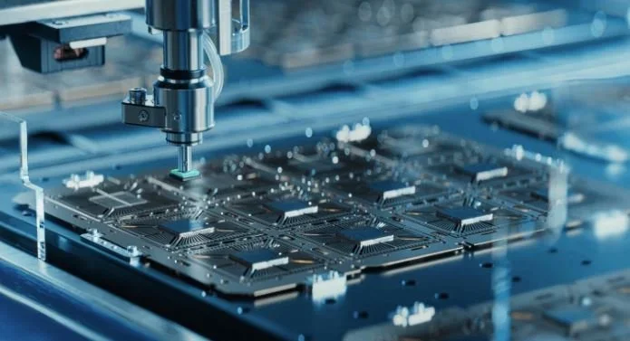
SK hynix is set to begin full-scale foundation work on its advanced packaging plant in Indiana, United States, by the end of this month. As competition in AI chips increasingly shifts toward advanced packaging capabilities, the company is moving quickly to strengthen its response to rising mid- and long-term demand for High Bandwidth Memory (HBM).
Industry sources reported on February 9 that SK hynix will start installing fencing at the construction site in West Lafayette, Indiana, from February 23, marking the start of preliminary work. From March 2, the company is expected to begin key preparatory activities for the main build, including ground grading, compaction and civil engineering work.
The Indiana facility, scheduled to begin operations in 2028, represents an investment of $4.09 billion. SK hynix recently applied for permits covering foundation work for several structures, including office buildings, a Central Utility Building (CUB), and the main semiconductor plant. With permits now being granted, construction momentum is accelerating. Industry observers expect official groundbreaking to take place in the first half of this year. An SK hynix spokesperson noted that the project is progressing step-by-step toward its 2028 operational target.
The plant will serve as a next-generation packaging hub for HBM, a crucial component in AI computing. SK hynix plans to begin mass production of its sixth-generation HBM (HBM4) this year and continues to hold a leading position in the global market. Forecasts suggest the company could supply around 70% of HBM4 used in NVIDIA’s upcoming AI accelerator platform, Vera Rubin.
Advanced packaging is a vital back-end process that directly impacts HBM yield and performance. With AI technology evolving rapidly, packaging has become a decisive factor in semiconductor competitiveness. As a result, major memory makers such as Samsung Electronics and SK hynix are intensifying efforts to enhance packaging expertise.
Beyond its U.S. expansion, SK hynix is also investing heavily in domestic infrastructure. The company plans to invest 19 trillion won (about $13.1 billion) in Cheongju, North Chungcheong Province, to build a dedicated Advanced Packaging & Test fab known as P&T7. Groundbreaking is expected in April, with construction completion targeted for the end of next year.

Project News