SemiCon Facility Requires Flexible Project Team
The 310,000 sq ft project is being delivered by a joint venture between Gilbane and DPS Advanced Technology Group
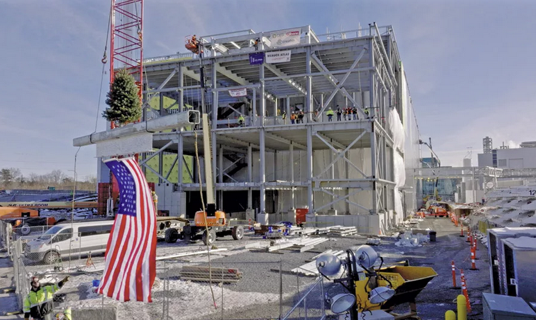
Construction is progressing on NanoFab Reflection, a major new nanotechnology research facility being developed at the existing semiconductor R&D campus in Albany, New York, with completion targeted for later this year.
The 310,000 sq ft project is being delivered by a joint venture between Gilbane and DPS Advanced Technology Group and represents the first major expansion of the NanoTech Complex in more than a decade.
One of the project’s biggest challenges has been designing the facility before final specifications for key semiconductor manufacturing equipment were finalised. The project team has therefore adopted a highly flexible approach to design and construction, ensuring the building can support both current and future generations of advanced chipmaking tools.
When complete, the facility will house a 200-ton semiconductor manufacturing system used for advanced ultraviolet lithography processes, alongside approximately 50,000 sq ft of ISO 5 cleanroom space designed to support evolving semiconductor technologies for decades to come.
Because the new facility is being built within an active semiconductor research campus operated by NY Creates, construction teams are also carefully monitoring vibrations and site activity to avoid disrupting ongoing research and development operations.
Nathan Speanburg, Senior Director of Construction at DPS, said the project requires balancing future-proofing, cost management and schedule certainty simultaneously.
“We are creating a highly adaptable facility capable of supporting technologies that may not yet even exist, while maintaining strict operational and construction requirements,” he said.
The four-storey development also includes a new 900-space parking structure and switchyard upgrades as part of a wider $614 million investment programme funded through New York State’s broader $1 billion semiconductor initiative.
The collaboration combines DPS’s specialist semiconductor engineering expertise with Gilbane’s extensive experience delivering complex projects across upstate New York. The project also reflects growing investment in advanced semiconductor research infrastructure as the US continues efforts to strengthen domestic chip innovation and manufacturing capabilities.

Project News