Start-up Lace raises $40m
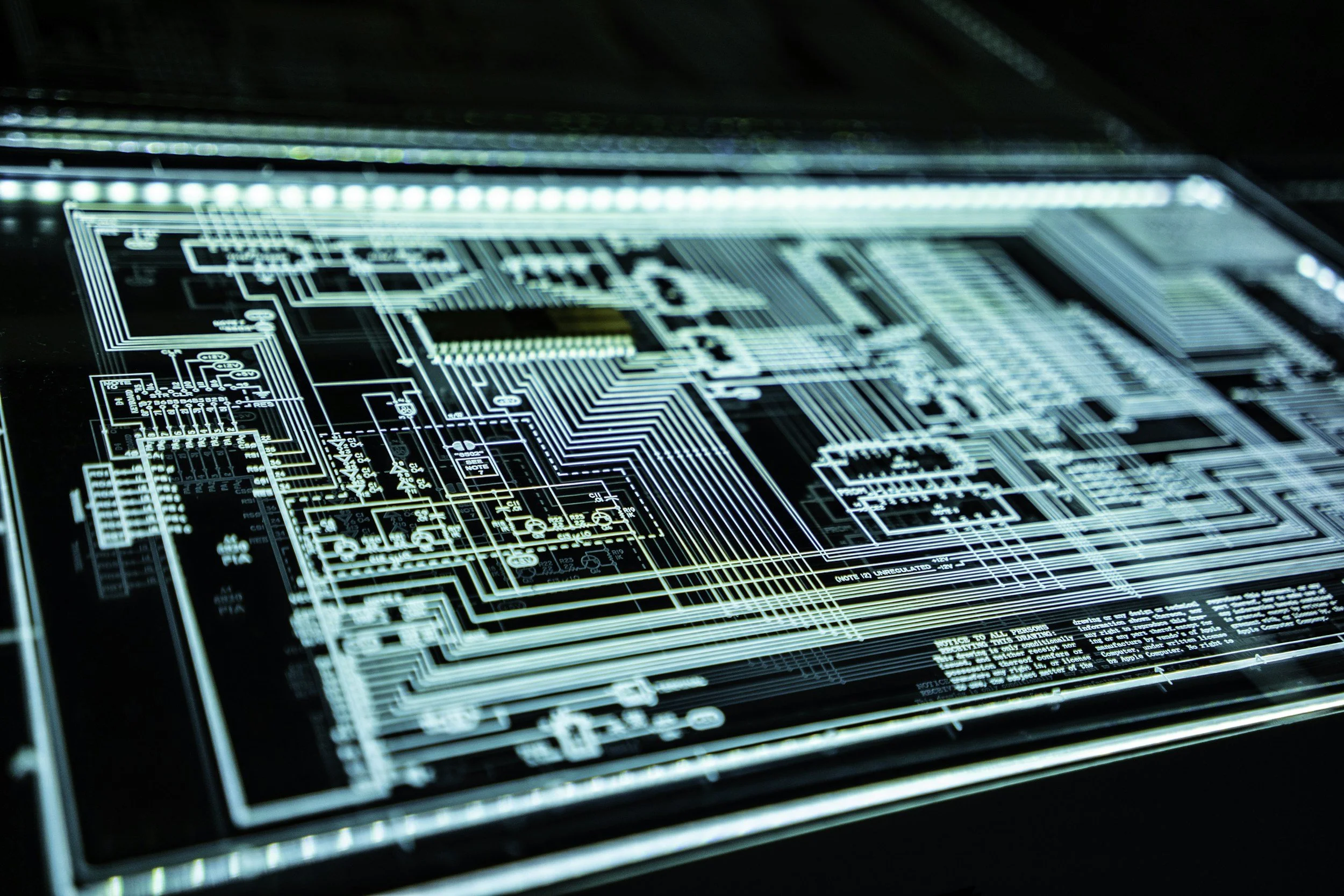
Traditional semiconductor manufacturing relies on photolithography
Lace Lithography, a Norwegian semiconductor equipment start-up backed by Microsoft, has secured $40 million in Series A funding to accelerate the development of its next-generation chip manufacturing technology.
The investment round was led by Atomico, with participation from M12, Linse Capital, Spanish Society for Technological Transformation and Nysnø.
Traditional semiconductor manufacturing relies on photolithography, where light is used to etch intricate circuit patterns onto silicon wafers. In contrast, Lace Lithography is pioneering a radically different approach using a helium atom beam. According to CEO Bodil Holst, this technology could enable chip features up to ten times smaller than those achievable today, opening new possibilities for advanced AI processors.
Experts highlight the potential of this method to push fabrication to near-atomic precision. John Petersen of IMEC noted that helium-based lithography could allow for feature sizes that are almost unimaginable with current techniques.
Founded in 2023 by Holst and Adrià Salvador Palau, the company is headquartered in Bergen, Norway, with additional operations in Barcelona, Spain. Prototype systems have already been developed, with plans to deploy a test tool in a pilot fabrication facility by around 2029.
Separately, Peter O’Brien of the Tyndall National Institute at University College Cork was recently honoured with the 2025 SEMI European Award, recognising his impact on global semiconductor innovation.

Project News